Fill out the form to talk to one of our PCB experts.
30+ Years of Experience
A Full Range of Rigid PCBs
Summit’s highly advanced manufacturing capabilities enable us to dependably build all types of PCB designs based on IPC standards. But we are never content with the status quo.
Our teams work alongside customers to push the boundaries of what is possible, helping to create truly astonishing electronic products.
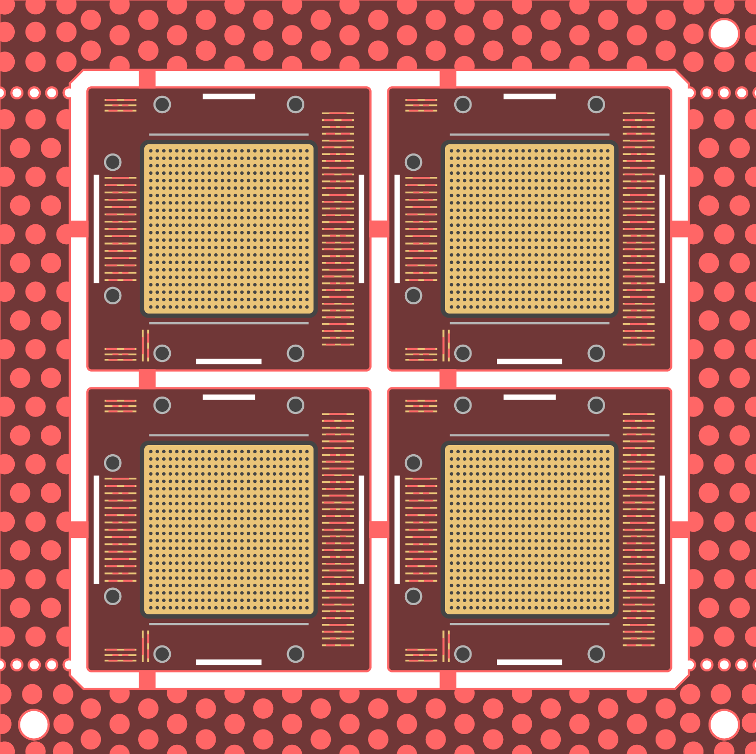
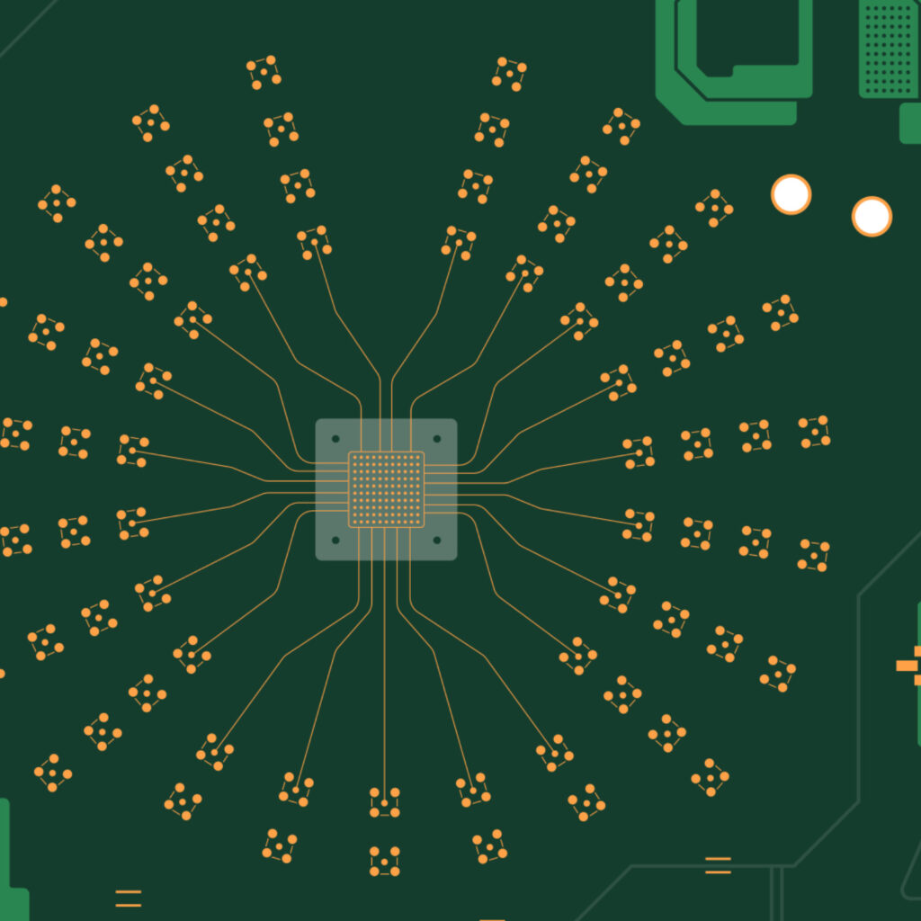
High-Density (HDI) PCBs
Due to the growing complexity of design structures, high-density circuit boards (HDI) are becoming essential in today’s electronics. As products increase in functionality and decrease in size and weight, circuit board designers need new solutions to maximize the space on each board.
For example, although blind and buried vias and vias-in-pad add complexity to the design, these features add more functionality without adding space.Summit Interconnect has the expertise and HDI technology to route highest density designs.
HDI designs typically include:
- Through vias from surface to surface
- Buried vias with through vias
- Two or more HDI layers with through vias
- Laser drill micro vias
- Passive substrate with no electrical connection
Rigid PCB capabilities highlights
- Multiple material options and surface finishes
- Blind, buried and micro via structures
- Stacked and staggered microvias
- Backdrilling
- Multiple sequential lamination
- Via fill (conductive and non-conductive)
- View all capabilities
We manufacture a broad range of PCB types and technologies for a one-stop solution
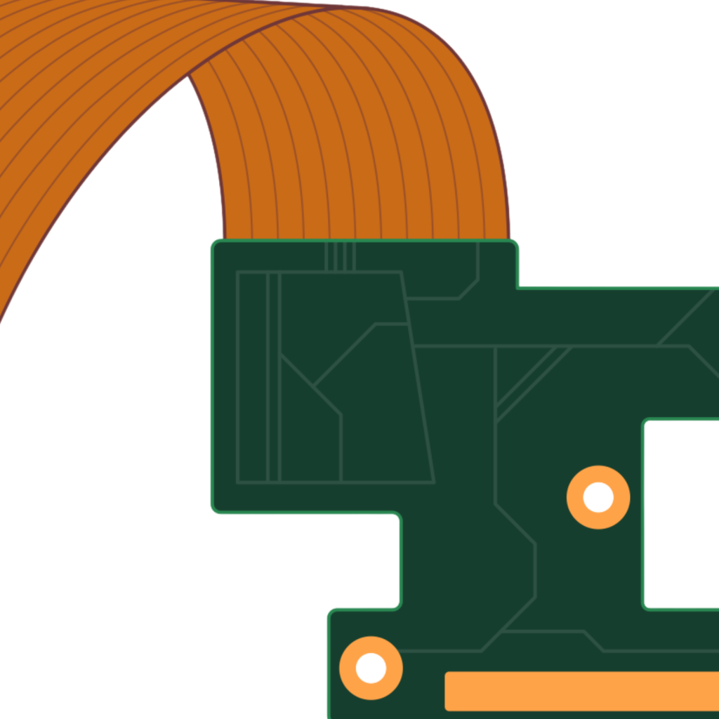
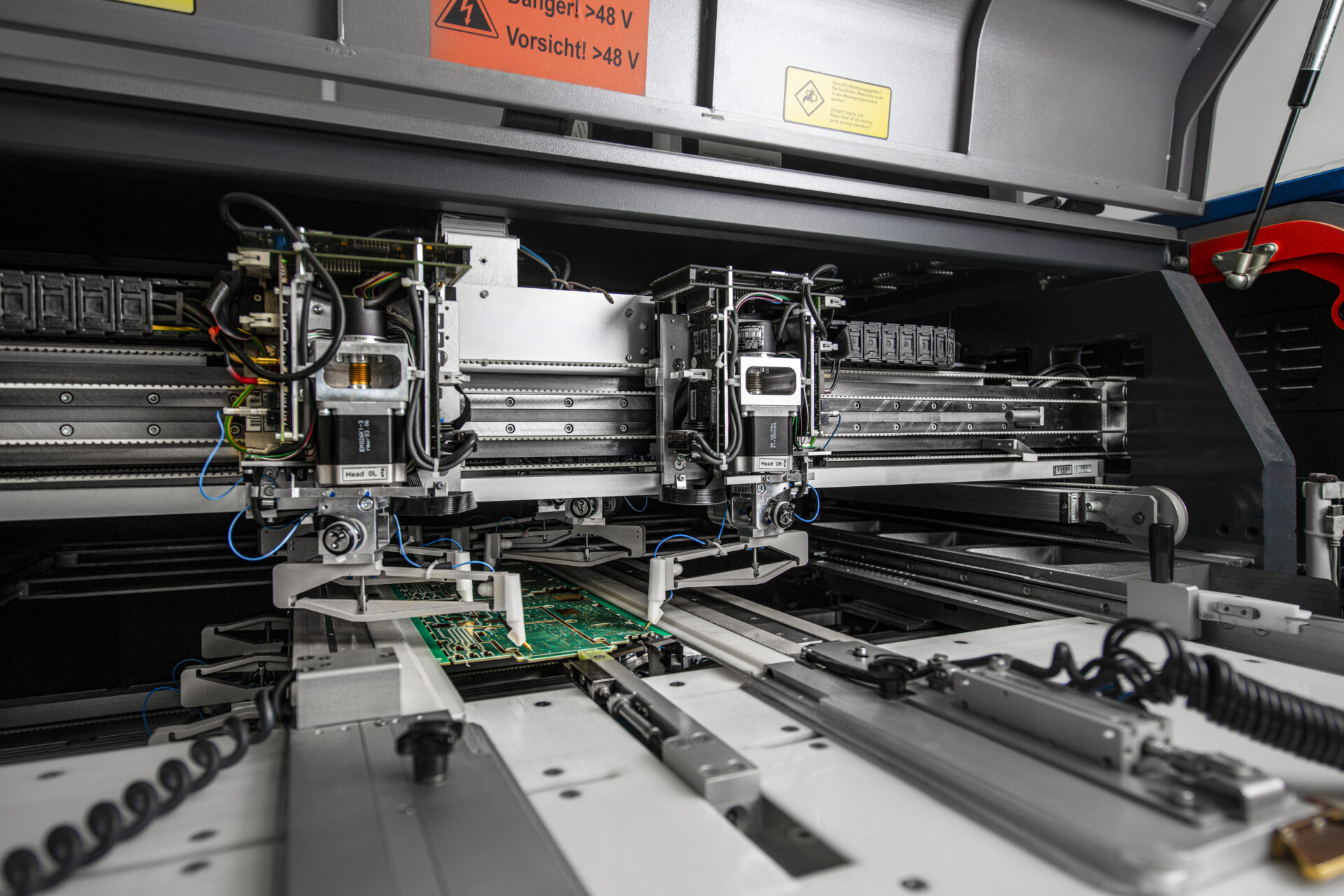
Rigid-Flex and Flex
As experts in rigid-flex and flex manufacturing, we handle rigid-flex, bookbinder, multilayer, adhesiveless u0026 adhesive, stiffeners, laser ablation, thin flex laminates, assembly options and more.
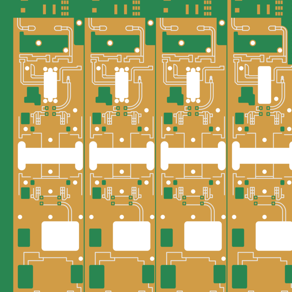
RF / Microwave
Our RF expertise includes using a wide range of PTFE materials, mixed material stackups, plated cavities, edge plating, high-temp lamination, mode suppression/stitching, buried resistors, and edge launch features.
Semiconductor
We specialize in semiconductor reference cards, probe cards, DUT, and burn-in-boards. Our RF capabilities include high aspect ratio, low-loss materials, bondable gold, tight tolerance drilling, and sintering.