The Process of Panelization in PCB Manufacturing and What it Means for Prototypes
Printed circuit board manufacturing can be a complex task, but with the right experience it can be done smoothly and efficiently. When it comes to PCB fabrication, a common manufacturing tool to use is panelization. Panelization refers to the grouping of boards for quicker processing.
What Is PCB Panelization?
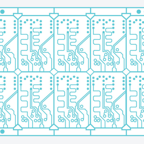
In high volume or quick turn orders, many PCB manufacturers will use panelization to optimize output. A fabricator will build blank boards to use in the manufacturing process. The designer will then find the best way to arrange the individual boards on a larger board, taking into account double-sided and multilayered PCBs as needed. Multilayered boards often come in 4, 6, 8, and 10 layers, but some circuit board designs can exceed 40+ layers for the most intricate electronic circuits. Creating the best arrangement can be difficult with circuit boards that need to fit in oddly shaped places, and therefore don’t follow a normal template.
The panel, also known as an array (depending on who you’re talking to), are then able to be processed as one large panel rather than several individual ones. In low volume PCB orders, panelization may not be needed, and the same is true for PCB prototypes. There are also certain restrictions on panelization such as thickness and space between boards as well as the overall weight. If a board could be compromised due to lack of strength, the design will have to be redone.
Understanding Depanelization
Once the boards are assembled and tested, they will need to be separated into their individual parts. There are many methods of depaneling PCBs, and which one you use depends on the type of panelization you chose. Panels can be created with either V-groove panelization or breakaway tabs, also referred to as tab-route panelization. V-groove panelization can only be used when there are no overhanging parts; it involves cutting a v-shaped line between the boards on both sides to minimize the thickness along a single track. Tab-route involves a method of perforation between the individual boards. Based on what type of panelization method was chosen, there are then different means of depanelization:
- Breaking by hand
- “Pizza cutter” along V-grooves
- Punching the boards out
- Depaneling Router
- Saw Cut
- Laser Cut
When discussing PCB fabrication and assembly with a circuit board manufacturer, find out what they’re able to do for you and what types of options they have when accommodating your design. Some companies are more than willing to allow for small batch testing before full orders are placed and offer other means of ensuring quality.
More articles
What is New in IPC-6012 Revision F?
IPC recently released an update to IPC-6012. Revision F covers qualification and performance specifications for ...
10 Causes of Lamination Voids and Ways Designers Can Prevent Them
One of the challenges in printed circuit board (PCB) manufacturing is the occurrence of lamination ...
How to Thoughtfully Design Embedded Cavities into a PCB
The increasing demand for compact, high-performance and reliable electronic devices requires novel solutions to address ...