
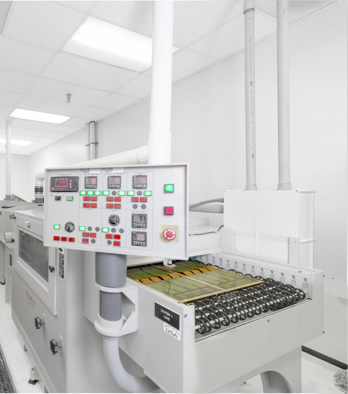
Lamination
From simple 2-layer boards to highly complex stack ups, we have the ability to fabricate all types of printed circuit boards.
| Board Details | Standard | Advanced | Emerging |
|---|---|---|---|
| Layer Count | 2-30 | 32+ | >48 |
| Minimum panel size | 12″ x 18″ | ||
| Maximum panel size | 18″ x 24″ | 21″ x 24″ | 24″ x 30″ |
| HDI layers | 2 – 3 | 4 | 8+ as permitted by laminate type |
| Sequential laminations | 2 – 3 | 4 | 8+ as permitted by laminate type |
| Layer-to-layer registration | +/- .002″ |
Thickness
Design and manufacturing factors usually determine the thickness of PCBs.
| Thickness | Standard | Advanced | Emerging |
|---|---|---|---|
| Minimum board thickness, single/double sided | .005″ | 002″ | |
| Maximum board thickness | .250″ | .300″ | |
| Minimum core thickness | .001″ | .0005″ | |
| Minimum core thickness (BC, Kapton) | .002″ | .001″ | .0005″ |
| Minimum prepreg fill | .003″ | .002″ | <.002" |
Drill and Mill
PCB drilling and milling creates holes, slots, and other cavities in an electronic circuit board.
| Drill and Mill | Standard | Advanced | Emerging |
|---|---|---|---|
| Minimum drill diameter, mechanical drill | .006″ | .005″ | .004″ |
| Mechanical drill aspect ratio, unfilled | 12:01 | 15:01 | 30:1 |
| Mechanical drill aspect ratio, filled | 10:01 | 11:01 | > 11:1 |
| Drill to metal (rigid) | .008″ | .007″ | .00525″ |
| Drill to metal (flex) | .012″ | .007″ | .00525″ |
| Drill edge to rigid flex transition | .100″ | .075″ | < .050" |
| Antipad diameter over drill size | .020″ + | .016″ | < .050" |
| Minimum class 2 annular ring, mechanical drill | .005″ | .004″ | <.004" |
| Minimum class 3 annular ring, mechanical drill | .007″ | .006″ | <.006" |
| Minimum drill diameter, laser micro via | .004″ | .003″ | <.003" |
| Microvia aspect ratio | 0.6:1 | 0.7:1 | >0.7:1 |
| Microvia capture pad / hole | +.007″ | +.005″ | +.004″ |
| Control depth drill tolerance | Keep back .010″ +/- .005″ | Keep back .005″ +/- .002″ | Keep back .004 +/- .0015″ |
| Back drill, diameter over primary drill | .008″ | .007″ | <.007" |
| Back drill anti-pad, diameter over primary drill | .016″ | .014″ | <.014" |
Etch Features
Copper is one of the most important elements in printed circuit boards. The current carrying capacity of a PCB depends on the thickness of the copper trace.
Copper traces are made by using chemicals to etch or remove copper from the board except where the wired connections are present.
| Etch Features | Standard | Advanced | Emerging |
|---|---|---|---|
| Minimum copper foil – internal | 1/2 oz. | 1/4 oz. | 1/4 oz. |
| Maximum copper foil – internal | 2 oz. | 4 oz. | 6 oz |
| Minimum copper foil – external | 3/8 oz. | 1/4 oz. | 1/4 oz |
| Maximum copper foil – external | 1 oz. | 3 oz. | >3 oz |
Inner and External Layers Print and Etch
Trace width and spacing requirements are based on the functionality of the circuit. They can affect electrical performance and signal integrity.
| Inner Layers | Standard | Advanced | Emerging |
|---|---|---|---|
| Minimum designed line width/spacing, 1/4 ounce foil | .002″ | <.002" | |
| Minimum designed line width/spacing, 3/8 ounce foil | .003″/.003″ | .0025″/.003″ | <.0025"/.002" |
| Minimum designed line width/spacing, 1/2 ounce foil | .004″/.004″ | .003″/.003″ | <.0025"/.002" |
| Minimum designed line width/spacing, 1 ounce foil | .005″/.005″ | .004″/.004″ | .0035″/.004″ |
| Minimum designed line width/spacing, 2 ounce foil | .008″/.008″ | .006″/.008″ | .006″/.006″ |
| Minimum designed line width/spacing, 3 ounce foil | .010″/.010″ | .008″/.010″ | .008″/.008″ |
| Plated External Layers | Standard | Advanced | Emerging |
|---|---|---|---|
| Minimum designed line width/spacing, 1/4 ounce foil | .0025″/.0025″ | .002″/.002″ | |
| Minimum designed line width/spacing, 3/8 ounce foil | .004″/.004″ | .003″/.003″ | .0025″/.003″ |
| Minimum designed line width/spacing, 1/2 ounce foil | .005″/.005″ | .004″/.004″ | .003″/.004″ |
| Minimum designed line width/spacing, 1 ounce foil | .006″/.006″ | .005″/.005″ | .004″/.005″ |
| Minimum designed line width/spacing, 2 ounce foil | .012″/.012″ | .010″/.010″ | .008″/.008″ |
| Copper fill to round feature spacing (donuts) | .006″ | .005″ | .005″ |
Soldermask
Soldermask is a thin layer of polymer that protects PCBs from oxidation and corrosion. It also helps avoid solder bridges and gives color to the board.
| Soldermask | Standard | Advanced | Emerging |
|---|---|---|---|
| LDI solder mask minimum web width, green color | .004″ | .003″ | less than .003″ |
| LDI solder mask clearance | +/-.002″ | +/-.0015″ | less than +/- .0015″ |
Legend
With more PCBs moving towards high-density, flex, and component miniaturization, the quality and readability of a legend is more important than ever.
| Legend | Standard | Advanced | Emerging |
|---|---|---|---|
| Inkjet legend printing | White | White | White |
| Color options | Green | Red, Blue, Black, White | Red, Blue, Black, White |
Mechanical
| Mechanical | Standard | Advanced | Emerging |
|---|---|---|---|
| Board profile dimensional tolerance | +/- .005″ | +/- .002″ | <+/- .002" |
| Plated through hole diameter tolerance | +/-.003″ | +/-.002″ | <+/- .002" |
| Non-plated through hole diameter tolerance |
+.002″/ -.001″ |
+/-.001″ | <+/- .001" |
| Flatness, warp and twist Per IPC-TM-650 2.4.22 | <.75% | <.5% BalancedConstruction | UnbalancedConstructions AABUS |
Impedance Testing
| Impedance Testing | Standard | Advanced | Emerging |
|---|---|---|---|
| Impedance controlled – single ended +/- % | +/- 10% | +/- 5% | <+/- 2% |
| Impedance controlled – edge couped diff. +/- % | +/- 10% | +/- 8% | <+/- 5% |
| Impedance controlled – broad side diff. +/- % | +/- 10% | +/- 8% | +/- 5% |
Electroplating
The electroplating process deposits metal onto the surface of the circuit board and inside the plated through-holes. The most common plated metal is copper.
| Electroplating | Standard | Advanced | ||
|---|---|---|---|---|
| Low Stress Nickel | 100 Microinches | 250 Microinches | ||
| Gold Plating Thickness | 30 Microinches | As Specified | ||
| Hole Aspect Ratio | 12 to 1 | 20 to 1 |
Finishes
The finish of a board, which is sometimes overlooked, is the interface between the board and the components that make the board function as desired.
| Finishes | Standard | Advanced | |
|---|---|---|---|
| HASL & HASL PB FREE | Yes | Yes | |
| White Tin | Yes | Yes | |
| Electroless Nickel/Palladium/Gold -ENEPIG | Yes | Yes | |
| Electroless Nickel/Immersion Gold – ENIG | Yes | Yes | |
| Immersion Silver | Yes | Yes | |
| Entek Plus HT/OSP | Yes | Yes |
Vias
Vias make electrical connections between layers on a printed circuit board. They can carry signals or power between layers. Summit specializes in advanced PCB technologies such as blind vias, buried vias, and via-in-pads.
| Types of Vias | Standard | Advanced | |
|---|---|---|---|
| Laser Micro Vias | .006″ | <.006" | |
| Blind / Buried Vias | .006″ | < .006″ | |
| Via in Pad | Yes | Yes |
| Via Fill | Standard | Advanced | |
|---|---|---|---|
| Non-Conductive ViaFill | Yes | Yes | |
| Silver / Conductive Epoxy Via Fill | No | Yes | |
| Copper Filled Vias | No | Yes | |
| Through Hole Copper Filled Via | No | Max 20 mils |
Inspection Processes and Options
Thorough testing and inspection occurs throughout the production process to ensure problems are captured early on, ensuring high quality and yield.
| Inspection Processes | Standard | Advanced | |
|---|---|---|---|
| Flying Probe Net List Test | Yes | Yes | |
| Impedance Control TDR | Yes | Yes | |
| AOI Inspection & Hi-Pot Testing | Yes | Yes | |
| Thermal Stress | Yes | Yes | |
| Peel Test | Yes | Yes | |
| Cross Section Pucks | Yes | Yes | |
| Solderability | Yes | Yes | |
| Impedance Coupons | Yes | Yes | |
| AB Coupon | Yes | Yes |
Panelized Board Size
Due to our advanced operational capacity and nearly limitless flexibility, we can assemble more PCBs faster than anyone else in the industry.
| Board Details | Standard | Advanced | |
|---|---|---|---|
| Board Size | .25″ x .25″ minimum size, panelized | 17″ x 21″ |
Processes
Our assembly facility utilizes the latest technology and equipment, and we always keep tabs on industry trends and customer demand to make sure our capabilities meet your PCBA needs.
| Assembly Processes | Standard | Advanced | |
|---|---|---|---|
| 3, 5, and 10-Day Turns | Yes | Yes | |
| Single-Sided SMT | Yes | Yes | |
| Double-Sided SMT | Yes | Yes | |
| Through Hole | Yes | Yes | |
| No Clean | Yes | Yes | |
| Clean / Wash | Yes | Yes | |
| ROHS and Leaded | Yes | Yes |
| Additional Assembly Processes | Standard | Advanced | |
|---|---|---|---|
| Press Fits | Yes | Yes | |
| Box Build | Yes | Yes | |
| Fine Pitch to 08 Mils | .08 Mils | .04 Mils | |
| BGA Repair and Reball | Yes | Yes | |
| Part Removal and Replacement | Yes | Yes | |
| Underfill | No | Yes | |
| Staking | No | Yes | |
| Conformal Coating | No | Yes | |
| Fencing and Shields | No | Yes |
Components
We provide full turnkey PCB assembly and manufacturing to help our customers across the country complete their projects on time. Our close and authentic partnerships with the most reputable US-based component and board suppliers is at the heart of the process.
| Components | Standard | Advanced | |
|---|---|---|---|
| SOIC | Yes | Yes | |
| QFP | Yes | Yes | |
| TQFN | Yes | Yes | |
| Leadless | Yes | Yes | |
| Through Hole | Yes | Yes | |
| LGA | Yes | Yes | |
| Passives | Down to 0201 | Down to 01005 | |
| BGAs, uBGA, and VFBGA | Yes | Yes | |
| Leadless Chip Carriers/ CSP | Yes | Yes | |
| Microelescronics | Yes | Yes | |
| Package-on-Package | Yes | Yes | |
| Flip Chips | Yes | Yes | |
| Hardware | No | Yes |
| Component Packaging | Standard | Advanced | |
|---|---|---|---|
| Cut Tape | Yes | Yes | |
| Loose Parts | Yes | Yes | |
| Reels | Yes | Yes |
Soldering Types & Methods
Soldering is one of the most basic techniques to understand for PCB assembly. Serving as a connective and conductive glue, a solid solder brings continuity and functionality to any circuit board.
| Soldering Options | Standard | Advanced | |
|---|---|---|---|
| Jet Paste Printing | Yes | Yes | |
| Stencil/Water Soluble Paste | No | Yes | |
| Vapor Phase Reflow | No | Yes | |
| Conventional Reflow | Yes | Yes | |
| Wave Solder / Selective Solder | Yes | Yes | |
| Programmable Selective Solder | No | Yes |
Inspection & Testing
Inspection is a critical part of the PCB assembly process. Without it, electronics manufacturers would never know for sure whether the PCB—and therefore the device—would work properly.
| Inspection Processes | Standard | Advanced | |
|---|---|---|---|
| Flying Probe | No | Yes | |
| 3D BGA X-Ray | Yes | Yes | |
| Functional Testing | No | Yes | |
| In-Line AOI | Yes | Yes | |
| Visual Inspection | Yes | Yes | |
| Component Inspection | Yes | Yes | |
| Component Value Check | Yes | Yes | |
| Ionic Contamination Test | No | Yes |
Quality Standards
Following quality standards ensures all aspects of a PCB design are correctly implemented and the end products perform exactly as expected.
| Quality Standards | Standard | Advanced | |
|---|---|---|---|
| AS9100D | Yes | Yes | |
| AS9102 FAIR | No | Yes | |
| IPC Class II | Yes | Yes | |
| IPC Class III | No | Yes | |
| ITAR Certified | Yes | Yes | |
| RoHS Compliant | Yes | Yes |
Depanelization Methods
Once the boards are assembled and tested, they will need to be separated into their individual parts. There are many methods of depaneling PCBs, and which one you use depends on the type of panelization you chose.
| Depanelization Methods | Standard | Advanced | ||
|---|---|---|---|---|
| V-Score | Yes | Yes | ||
| Mouse Bites | Yes | Yes | ||
| Mechanical Routing | No | Yes |